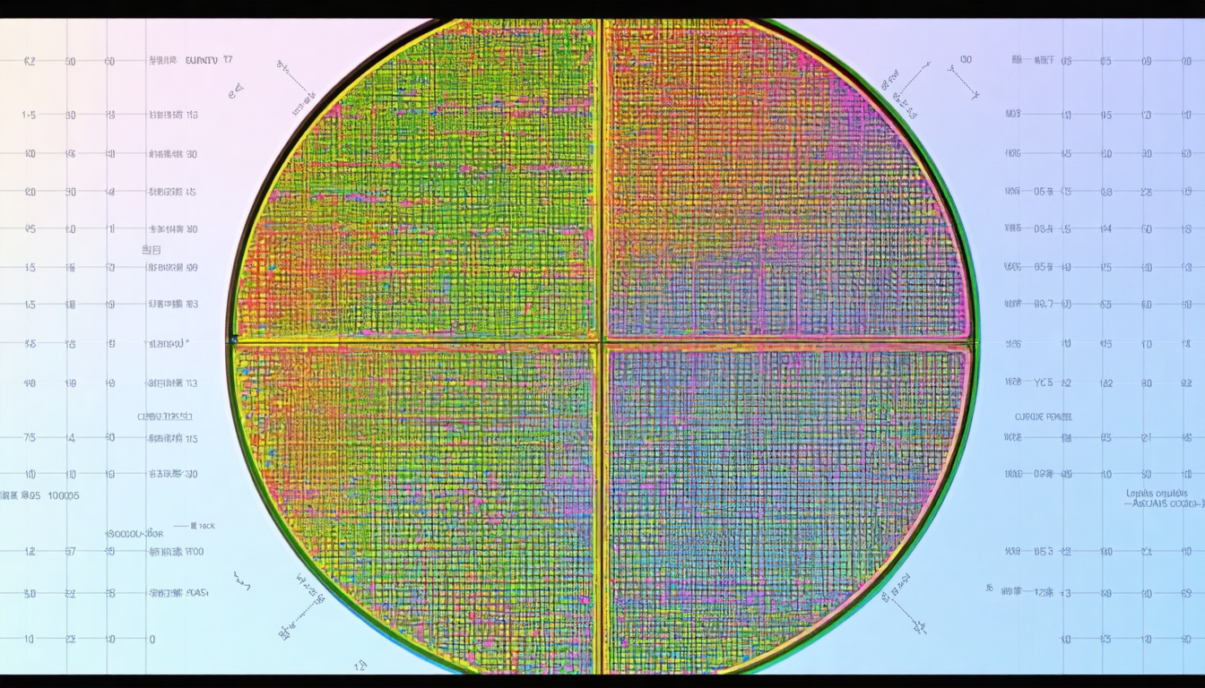
A yield engineer who can read spatial patterns on wafer maps quickly narrows the root cause candidate list before pulling a single equipment log. This skill is as important as knowing which defect types are yield-killers, and it is less systematically taught. Most process engineers develop it through years of experience looking at wafer maps and correlating patterns to confirmed root causes. The goal of this post is to make that pattern library explicit.
Why Spatial Position Is a Root Cause Signal
Semiconductor process equipment has spatial non-uniformity by design. Deposition tools have deposition rate profiles that are higher at center or edge depending on the chuck geometry and gas distribution design. Etch tools have etch rate profiles shaped by plasma density distribution and gas flow. CMP tools have pressure profiles determined by the polishing head geometry and the platen speed differential. Every process step leaves a spatial fingerprint on the wafer.
When a process parameter drifts outside its control envelope, the resulting defect pattern often has the same spatial signature as the underlying process non-uniformity. An etch tool whose center-to-edge etch rate ratio shifts will produce defects that concentrate at the center or edge of the wafer in a pattern consistent with the direction of the shift. That spatial signature persists even at downstream inspection steps, because the physical damage was done at the etch step. Reading the pattern at the downstream step tells you where to look upstream.
Edge Ring Patterns
Edge ring patterns — elevated defect density in a band around the wafer perimeter, typically 3mm to 10mm from the edge — are among the most common spatial patterns encountered in 300mm fab work. The most frequent root causes fall into three categories.
The first is bevel particle contamination. Particles accumulate at the bevel edge of the wafer during transport and handling, and can redistribute to the wafer surface during thermal processing. Edge ring defect density that increases after anneal steps and decreases after wet cleans is characteristic of this mechanism. The fix is typically a bevel etch program combined with more frequent carrier cleaning.
The second is edge seal ring breach in deposition steps. During CVD and ALD deposition, the edge of the wafer is mechanically supported by a ring or edge exclusion zone. If the seal degrades, precursor gas reaches the wafer edge inconsistently, producing non-uniform film thickness at the edge that appears as a defect cluster at downstream inspection. This pattern is distinguished by its very sharp inner boundary — typically a nearly perfect circle at a consistent radius.
The third is CMP edge non-uniformity. CMP polishing pressure is often highest at the wafer edge because of the retaining ring geometry. Over-polishing at the edge produces surface roughness that appears as an edge ring of apparent defects at the optical inspection step. This pattern has a softer inner boundary than the seal ring pattern, and the density gradient is usually gradual rather than step-like.
Center Spot Patterns
A center spot — elevated defect density in a roughly circular region at the wafer center — most often points to process chuck or carrier pin contact issues. In most process chambers, the wafer rests on pins or a chuck with center-heavy support geometry. If the support surface is contaminated or worn, the contact points transfer contamination or stress to the wafer surface in a pattern that concentrates at center.
Center spots are also characteristic of certain plasma etch conditions where the plasma density peaks at center, producing center-high etch rate that over-etches sensitive layer interfaces. The distinction between contact contamination and plasma non-uniformity usually requires cross-referencing with the process step: a center spot that appears specifically after a plasma etch step, with no equivalent at prior inspection steps, points to the plasma mechanism. A center spot that persists from an inspection before the etch step was run points to something earlier in the lot history.
Scratch and Arc Patterns
Scratch patterns — linear or arc-shaped tracks of elevated defect density that cross multiple die — are almost always handling-related. The most common sources are: wafer cassette slots with worn or contaminated contact points, FOUP (Front Opening Unified Pod) door mechanisms with particle generation issues, robot end-effector edge wear, and aligner pin damage. Scratch patterns that follow a consistent arc shape across multiple wafers from the same cassette slot are the signature of cassette damage.
The distinction between a mechanical scratch and a process-induced scratch is usually made by reviewing the CDSEM images at the scratch location. Mechanical scratches show surface gouging and particle redistribution along the track. Process-induced linear patterns (for example, from non-uniform gas flow in a CVD chamber) show different morphology — surface texture changes or film thickness variation rather than physical gouging.
Half-Moon and Notch-Relative Patterns
Defect patterns that are consistently positioned relative to the wafer flat or notch — same angular position, same radial distance, across multiple wafers — are equipment-specific signatures rather than process non-uniformity signatures. They indicate a specific mechanical element in the process chamber that contacts or affects the wafer at that position: a pin, a clamp, an edge contact point, or a gas inlet that is positioned asymmetrically.
These patterns require wafer orientation normalization before they are visible. If wafers are loaded with random orientations in different lots, the notch-relative signature will average out in aggregate wafer map statistics and appear as random noise. SynthKernel normalizes all wafer maps to a standard notch-up orientation during ingestion, which makes notch-relative signatures visible in wafer-to-wafer comparisons. This normalization step is the reason we can detect equipment signatures that are invisible in non-normalized defect density statistics.
Ring Plus Center Combinations
Some process excursions produce compound patterns — an edge ring plus an elevated center, or a ring at an intermediate radius plus elevated center. These combinations are often characteristic of deposition uniformity changes. A precursor gas flow change that simultaneously affects the center flow and the edge seal behavior can produce this pattern. CVD tungsten processes are particularly prone to this when the gas flow controller for the main reactant gas has a sticking valve — the result is an oscillation in precursor concentration that affects both the center and edge zones of the deposition profile simultaneously.
Using Spatial Pattern Matching in Automated Analysis
Pattern-to-root-cause matching can be systematized. The SynthKernel spatial analysis engine extracts quantitative spatial features from each wafer map — radial defect density profile, angular distribution relative to notch, cluster eccentricity, and inner/outer boundary sharpness — and compares them against a library of pattern archetypes built from confirmed root cause events in the historical database.
The comparison produces a ranked match list: "this wafer map matches the spatial signature of bevel contamination at 89% similarity, CMP edge over-polishing at 67% similarity, and plasma etch center-high non-uniformity at 42% similarity." Those similarity scores drive the root cause candidate ranking, weighted by the defect type classification from the CDSEM review step and the process step where the pattern first appeared.
The practical result is that a yield engineer responding to an excursion alert receives not just "elevated defect density at M1 optical inspection" but "edge ring pattern at 5mm radius, consistent with bevel contamination history from three prior events in the last 90 days, check carrier cassette slots 12-18 on carrier CARR-0042." That specificity changes the engineer's first action from pulling a broad equipment history query to inspecting a specific carrier — which is a 10-minute check rather than a two-hour analysis.
The Limits of Pattern Matching
Spatial pattern matching works reliably for excursions that fit established archetypes. It is less reliable for novel failure modes — new process steps, new materials, or first-occurrence equipment failures with unusual spatial signatures. In those cases, the pattern matching engine will produce low confidence scores and route to human review. That routing is the correct behavior; forcing a low-confidence match to a historical archetype would produce misleading root cause suggestions. The goal is to automate the high-confidence cases and preserve engineer attention for the genuinely novel ones, not to eliminate human judgment across the board.