Process yield problems are expensive. They cost more when the root cause stays hidden for three shifts.
Before SynthKernel, our founding team spent a combined 22 years in process engineering and yield analysis at three different CMOS logic fabs. The tool we needed — one that could automatically correlate defect signatures from inline inspection to electrical fail patterns at probe — didn't exist in the form we needed it. Vendor solutions were either narrowly scoped to one tool type, required weeks of custom scripting to connect to our MES, or produced outputs that required a data scientist to interpret before a yield engineer could act.
The breaking point was a 28nm SRAM excursion in late 2022. We had the inspection data on the morning of Day 1. The root cause — a chamber mismatch on an etch tool that had been running 11% outside spec — wasn't identified until Day 4, after three additional lots had processed through the same tool. Total yield impact: 17 wafers, partial loss across four lot numbers. The information to catch it earlier existed. No tool was connecting it fast enough.
SynthKernel was founded in 2024 with one goal: make the 12-minute alert we demonstrated in our first internal proof-of-concept the standard response time for any yield excursion in any fab that runs modern inspection equipment. We're a team of eight, based in Menlo Park, and we've run proof-of-concepts at three fab sites since incorporation.
Team members across process engineering, ML, and systems integration
Fab sites where pilot deployments are currently running
Defect type categories in our pre-trained classification library
Founded in Menlo Park, CA — currently at Seed stage
An alert without supporting evidence just creates a task. We measure ourselves on how quickly a yield engineer can confirm or rule out a hypothesis with data already in front of them — not on how fast we fire a notification.
We integrate with the equipment and systems already in production — KLA, Lam, ASML, your MES, your SPC charts. Adding SynthKernel should not require a process change review or a change control committee approval just to connect it.
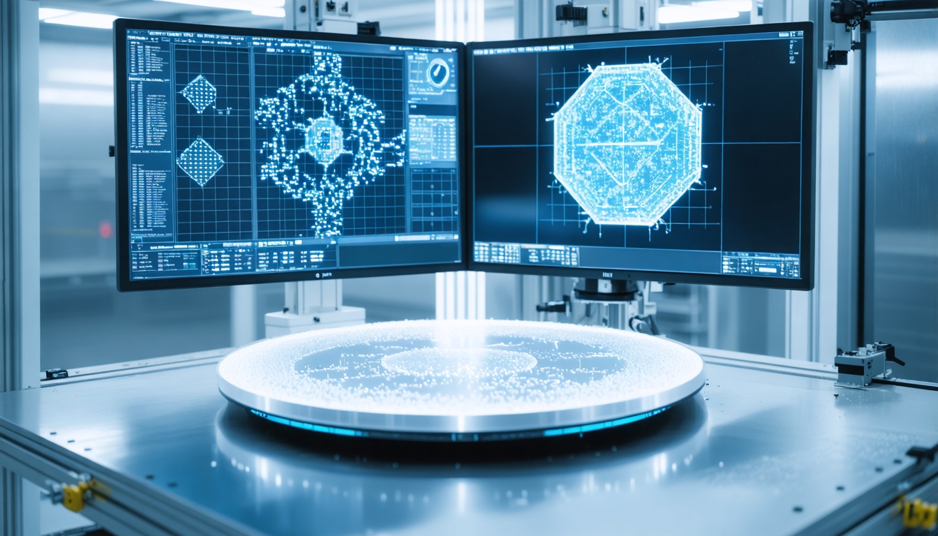
Wafer images contain process IP that took decades to develop. We run every model inference on-premise, with no outbound data transfer required. Not for updates, not for retraining, not for telemetry. That's an architecture decision, not a marketing claim.
Three proof-of-concept deployments, three distinct fab environments, same pattern: faster root cause, fewer affected lots per excursion.
Time-to-root-cause reduced from 41 hours to 19 hours across three excursion events tracked during the pilot. Etch chamber matching issue identified on Day 1 of the third excursion — previously would have required two days of manual log review.
Containment improved: during the pilot period, average affected lot count per excursion dropped from 9 to 4. Optical review spatial pattern detection caught a recurring scratch signature tied to a CVD lift-pin before it generated a yield report at probe.
Alert to disposition time reduced from 28 hours to 11 hours for particle contamination events. Lineage tracking identified the specific incoming wafer carrier batch as the contamination source — information that was available in the MES but had never been connected to the inspection output automatically.
Talk directly with one of our founding engineers. Not a sales rep — someone who built the system and has run yield analysis in production.