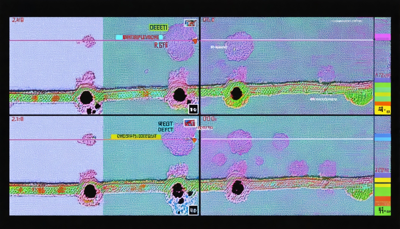
Inspection tools produce a map. A yield problem produces a pattern across maps. These two statements seem obvious but they describe a gap that costs fabs significant engineering time every quarter. Most fab yield analysis workflows are organized around individual inspection layers — you review the optical scan output from after etch, the CDSEM images from the review step, the metrology readings from after CMP. Each layer tells you something. What they tell you together is almost always more important than what any one of them tells you alone.
The Layer Isolation Problem
The practical reason yield analysis stays layer-by-layer is organizational. KLA Surfscan output goes into one database. Lam etch endpoint data goes into the MES. CDSEM images live in the defect review system. WAT results come from the probe tester and feed into a separate yield management system. The data is in different formats, different schemas, and different tools maintained by different equipment support teams. Correlating across them requires either a custom data pipeline or a lot of manual export-and-compare work in Excel.
This is not a data volume problem. Most 300mm fabs generate between 50 and 200 GB of inspection data per day — manageable by any modern analytics infrastructure. The barrier is schema alignment and the absence of a common wafer identifier that persists across tools. Different equipment vendors use different lot ID formats, different wafer numbering conventions, and different timestamp precision. Joining a KLA KLARF file to a Lam etch log requires resolving those mismatches first.
What Gets Missed When Layers Are Analyzed Independently
Consider a scenario common in logic fabrication: a bridging defect type appears on the post-Metal-1 inspection step with elevated density in the top-right quadrant of affected wafers. Analyzed in isolation, the responsible team logs it as a Metal-1 etch issue and schedules a process chamber inspection. The etch chamber looks clean. The issue persists. Three weeks later, someone pulls the prior CMP data and notices that the same quadrant showed elevated non-uniformity on the inter-layer dielectric CMP step that preceded Metal-1 deposition.
The CMP roughness created a subtle topography variation that changed the local etch rate during the Metal-1 etch step. The root cause was CMP non-uniformity. The symptom appeared at Metal-1. The yield engineer looking only at the Metal-1 inspection map was solving the wrong problem, and the CMP engineer looking only at CMP metrology saw nothing that triggered an alert. Neither analysis was wrong given the data available to it. Both were incomplete.
Spatial Correlation as the Primary Signal
The most reliable early indicator of a cross-layer yield problem is spatial pattern correlation. When the same wafer location produces elevated defect density or metrology deviation across two or more consecutive inspection steps, the root cause almost always originates at or before the earliest step in the sequence. The later steps are reproducing the pattern because they are responding to a surface condition inherited from upstream.
Spatial correlation analysis requires registering defect coordinates from different inspection tools to a common wafer coordinate system. This is non-trivial because different tools have different stage resolutions, different notch orientation conventions, and different reference mark placement. KLA's Klarity and Synopsys Yield Explorer both have built-in coordinate registration capabilities, but they require that the data already be loaded into those systems. For fabs that have not completed data integration at that level, coordinate registration has to happen at the analytics layer.
SynthKernel handles coordinate normalization during ingestion, converting all inspection coordinates to a standardized wafer-space reference frame before any correlation analysis runs. This is what enables cross-tool comparison without requiring the customer to maintain a unified inspection database schema in their MES.
Time-Shifted Correlation Across Non-Adjacent Layers
Direct layer-to-layer correlation captures the most obvious cases. Harder to detect — and often more damaging — are yield effects where the root cause and the symptom are separated by multiple process steps and significant time. A contamination event at the front-end shallow trench isolation (STI) etch step, for example, can produce a yield signature that does not appear clearly until electrical test at probe, with 60 to 90 days of additional processing in between.
Catching these time-shifted correlations requires maintaining defect history across the full lot process history, not just the most recent inspection cycle. That means indexing by wafer serial number and equipment ID, not by lot snapshot time. It also means keeping inspection data accessible over the full process timeline, not archiving it after the lot is completed. Data retention policies at many fabs archive inspection data 30 to 60 days after lot completion — which is often before probe results are available. That gap makes retrospective root cause analysis for long-flow lots nearly impossible.
Defect Density vs. Defect Position: Why Both Matter
Two wafers can have identical defect density on the post-etch inspection and very different probe yields. The difference is usually defect position relative to critical layers and device features. A 0.15-micron particle on open field oxide is benign. The same particle bridging two metal lines at a critical spacing is a hard kill. Defect density as a metric flattens this distinction.
Defect-limited yield models like the negative binomial model — which most fabs use for yield prediction — incorporate both density and clustering parameters, but they still operate on a per-layer basis. The yield-limiting combination is often a moderate density at two adjacent layers landing on overlapping device regions, not an extreme density at a single layer. That combined effect only becomes visible when you are looking at both maps simultaneously and registering defect positions to the design layout.
Practical Implementation: Where to Start
For fabs starting to build multi-layer correlation capability, the highest-value first step is usually connecting post-etch inspection data to the immediately preceding metrology step for the same layers. Start with the two or three process steps that have historically contributed the most yield loss, and build the correlation pipeline for those before expanding. This keeps the initial implementation scope manageable and produces visible results quickly enough to justify continued investment.
The second step is connecting inline inspection data to probe yield results, even if only for representative wafer sample sets initially. The probe-to-inspection correlation — even done retrospectively on historical data — is typically the fastest way to identify which inspection defect types actually kill devices versus which ones are cosmetically elevated but electrically benign. That filter alone can dramatically reduce the number of excursion alerts that require engineering investigation.
What Multi-Layer Correlation Does Not Solve
Multi-layer correlation is a diagnostic tool, not a process control tool. It tells you what happened and where it originated after the fact. It does not prevent the next occurrence. Closing that loop requires feeding correlation insights back into APC set points and SPC alert thresholds — which is a different problem involving different systems and different organizational commitments. The diagnostic speed gain from good multi-layer correlation is real and significant, but it has to connect to an action pathway to produce consistent yield improvement rather than just faster root cause writing.
The correlation capability also degrades when data quality is inconsistent. If the CMP metrology tool has a known offset that has not been corrected, or if the CDSEM review sampling rate is too low to give a statistically meaningful defect map, the correlation will be misleading. Good data hygiene is a prerequisite. The AI classification and correlation models we use at SynthKernel can handle some measurement noise, but they are not a substitute for maintaining calibrated, consistently sampled inspection data across the process flow.
A Different Way to Think About Inspection Investment
Most fab conversations about inspection investment center on individual tool capability: what defect size can this scanner detect, what is its throughput, how does its image resolution compare to the previous generation. Those are the right questions for tool procurement. They are incomplete questions for yield program design. The value of any individual inspection step depends not just on what it can detect but on how well its output integrates with every other data source in the correlation chain.
A lower-resolution optical scanner whose output is fully integrated into a cross-layer correlation pipeline can contribute more to yield improvement than a higher-resolution scanner whose data sits in an isolated review workstation that no one queries systematically. The analytical architecture matters as much as the instrument specification. That is not an argument against investing in better inspection tools — it is an argument for making the analytical infrastructure a first-class investment alongside the tools themselves.